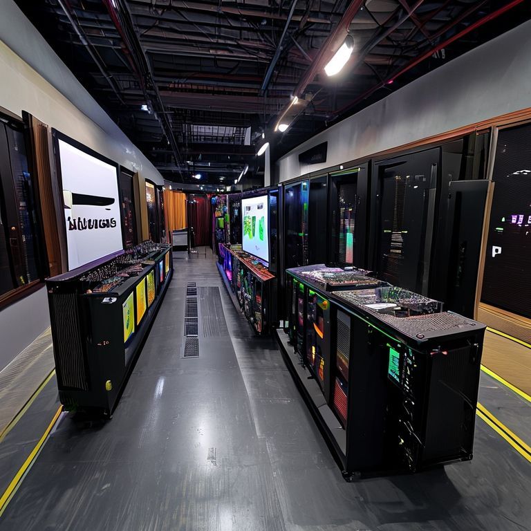
AMD Unveils Venice Server CPU and MI400 Accelerator at CES 2026
At CES 2026 AMD showcased its Venice server CPU and MI400 accelerator, revealing new chiplet-based architectures that push silicon efficiency and core count. Venice employs a dual‑IO die layout and advanced packaging reminiscent of the Strix Halo, while the MI400 features 12 HBM4 dies and extensive compute chiplets. These innovations position AMD to power next‑generation data‑center workloads and AMD’s Helios AI Rack.
AMD unveiled two cornerstone silicon products at the 2026 Consumer Electronics Show (CES) – the Venice series of server CPUs and the MI400 family of data‑center accelerators. While the company had first outlined technical specifications for Venice and the MI400 at its June 2025 “Advancing AI” event, this was the inaugural live presentation of the actual silicon.
**Venice – A Chiplet‑Based Server CPU**
Venice departs from AMD’s prior EPYC Rome design by moving to a more sophisticated form factor that reduces reliance on the organic substrate used to interconnect chiplets. The new packaging resembles the Strix Halo (used on MI250X), with 165 mm² silicon per core chiplet (CCD). Each CCD contains 32 Zen 5 cores and 4 MB of L3 cache per core, yielding 128 MB of L3 per CCD – a total of up to 256 cores across eight CCDs.
Unlike earlier EPYC chips, Venice incorporates two IO dies instead of one. Each IO die is roughly 353 mm², for a combined silicon area of just over 700 mm²—an increase from the 400 mm² dedicated for IO on previous EPYC processors. The IO dies are arranged under the CCDs, connected by a die‑to‑die interface that minimizes latency and improves power delivery. Surrounding the IO dies are eight ancillary dies, four on each side of the package, which likely serve as structural silicon or deep‑trench capacitors to sustain voltage stability across the high‑core‑count workload.
**MI400 Accelerator – Expanding Compute and Memory**
The MI400 accelerator builds on AMD’s earlier MI350 architecture but expands in several dimensions. It is a large package that integrates 12 HBM4 memory dies alongside two base compute dies fabricated at 2 nm and 3 nm nodes. Two extra dies on the top and bottom of the base dies handle off‑package I/O, including PCIe and UALink connections.
A rough die‑area calculation shows each base die at about 747 mm², with the off‑package IO dies at ~220 mm² each. The compute chiplets are divided across the two base dies; while the factory has not released exact figures, estimates place each compute die at 140–160 mm², with the entire compute block not exceeding 180 mm² in total.
**Broader MI400 Family and Venice‑X**
In addition to the newly revealed MI400 models, AMD announced a third member, the MI440X — a direct replacement for the MI300/350 series that is optimized for 8‑way UBB chassis. The MI455X and Venice processors will feed the Helios AI Rack, a next‑generation platform poised to deliver both high core counts and advanced AI inference.
Venice‑X is also on the horizon, expected to be a V‑Cache extension of Venice. If AMD continues its current cache ratio, a 256‑core Vega‑5 core chiplet could support up to 384 MB of L3 cache per CCD, translating to roughly 3 GB of L3 cache across the entire chip.
**Looking Forward**
Both Venice and the MI400 series are slated for launch later this year, and the industry is eagerly awaiting deeper insights into their internal architectures. AMD’s move toward more integrated, package‑level solutions marks a significant step in delivering higher performance while maintaining power efficiency.
For more in‑depth coverage and community discussion, contributors are encouraged to support the publication on Patreon or PayPal, and join the official Discord channel to engage with fellow experts.